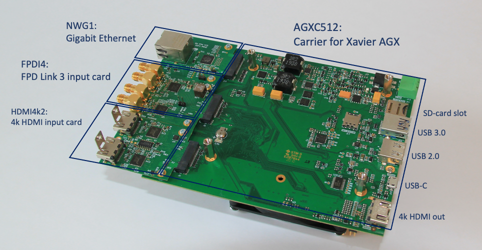
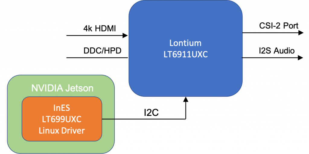
Running artificial intelligence (AI) algorithms, such as neural networks, directly on embedded devices has many advantages compared to running them in the cloud: One can save significant amounts of cloud storage, reduce power consumption and enable real-time applications. In addition, privacy is increased and required bandwidth reduced because only the AI algorithms results are forwarded to the cloud, not the full data. However, setting up the environments for custom neural networks on embedded devices can be difficult. Thats why the HPMM team provides a fully “dockerized” reference workflow for the Nvidia Jetson Nano. It includes:
Container to convert Tensorflow and Pytorch models to .onnx models
Container to cross-compile a C++ TensorRT applications for a Jetson Nano including opencv
Container to run TensorRT networks on the Jetson Nano with the C++ and Python API
Please find the link to the reference workflow here.
If you are interested in running AI algorithms on microcontrollers, such as the Cortex M4, we provide the reference workflows for several frameworks such as TensorFlow lite for microcontrollers, CMSIS-NN and ST CUBE AI here.
Feel free to contact us regarding your custom application or project regarding embedded artificial intelligence!
The Institute of Embedded Systems (InES)High Performance Multimedia group generated a low latency version of the classic Jamulus music rehearsal application for the Raspberry Pi 4
The classic Jamulus is an open source application for music groups who want to rehearse over the internet. Especially with the global pandemic, Jamulus is a great solution for bands and choirs to rehearse from home. With the Jamulus-Direct solution, the Institute of Embedded Systems reduces the latency of the audio connection compared to the classic Jamulus. The low audio latency is achieved through multiple peer-to-peer connections. This means that each participant is connected to the other members of the group via a dedicated connection. The audio no longer needs to be sent via an audio server, which reduces the latency.
Peer-to-Peer communication in Jamulus Direct reduces latency
The figure below shows the audio transmission in a classical server based session with three clients. Three computers run a client software. Computer 0 starts a client and a server. Each client sends their own audio to the server. The audio is mixed together at the server and sent back to the clients. However, the server topology shown below introduces latency because all data has to make a detour over the server.
No peer-to-peer communication in classical Jamulus introduces latency
Therefore, in Jamulus direct, a peer-to-peer topology eliminates the detour via the server (see figure below). Each participant in a peer-to-peer system exchanges its data with each other participant. Peer-to-peer is therefore the preferred structure to achieve the lowest possible latency.
Peer to peer connections between three clients
This setup ensures the lowest possible latency between each device. To achieve low latency, a few challenges had to be mastered to get a well functioning system. For instance, that peer to peer connections usually are blocked by the firewall of the network router and therefore need a mechanism to open these ports on the firewall. A further issue is the management of the session. In server based systems, the server usually manages the session. It is the contact point for new clients to register to join the session and also to unregister when leaving. The peer-to-peer audio transmission showed audio latencies under 30 milliseconds for two locations, with a ping time of 13 milliseconds. A detailed paper of Jamulus Direct can be downloaded here.
Jamulus-Direct is written for the Raspberry Pi 4 and achieves high quality audio utilizing a USB audio card connected via the RPI4 USB interface. Every audio card with available Linux drivers is suitable (Tested with Focusrite Scarlet 2i2 and Behringer U-Phoria UM2)
The Institute of Embedded Systems (InES) at ZHAW, with great experience in hardware development for NVIDIA computing modules, is now shipping its modular vision system based on high-performance NVIDIA Xavier AGX.
To shorten the time to market, the prototyping system consists of a greatly reduced motherboard that can be equipped with different types of M2-footprint modules to add functions like HDMI in and out, FPD-Link III in and out, USB-c etc.
Due to the modular architecture, the user may configure a personalized system by adding from a choice of different modules. Due to the low complexity and flexibility of the provided interfaces, more custom-made modules can easily be developed.
FPDI4: FPD-Link III deserializer card with 4 inputs
USBC2: USB-C card with 2 x USB-C
NWG1: GBit Ethernet card
The system consists of a minimal mother board, which only includes the necessary circuitry to startup and program the Xavier.
To keep size and costs low, the main board includes USB 2.0, HDMI and one 16-lane PCIe standard card slot. All other interfaces are provided by nine PCIe M2-footprint sockets which share not only PCIe lines, but also dedicated Xavier-AGX interfaces like MIPI- CSI, USB and I2C. An overview of possible configurations and currently available devices is given in the table below.
Front view with Nvidia-Xavier-AGX on topSlot connections to Xavier and currently available ModulesModules may easily be exchanged
The Video-Out socket provides two HDMI or DisplayPort lines, as well as the required I2C lines. It is also possible to configure one DisplayPort and one HDMI output. This slot also carries USB2.0, if the user wants to implement HD-BaseT.
The USB socket allows two USB interfaces with USB connectors of choice (USB-A-B-C, USB on the go) I2C, CAN-Bus and serial UART are also supported.
Video-In Module 1 and 2 each support 2 CSI ports with 4 lanes or 4 CSI ports with 2 lanes which allows connecting 4k cameras or HDMI to CSI converters
The Network Module allows the connection of 1GBIT Ethernet over RGMII or another PCIe lane for PCIe high speed PHYs
Available Modules for Xavier prototyping board
For more information, availability and pricing, please see contacts on the right.
The ZHAW Institute of Embedded Systems (InES), High Performance Multimedia Group, developed a 4k video for Linux driver for the Lontium LT6911UXC HDMI to MIPI CSI-2 converter IC. The driver was written for NVIDIA Jetson Processors and enables the following features of the LT6911UXC
Supports 4k HDMI 2.0 to MIPI CSI-2, requiring only one CSI port
Up to 4k resolution
Only 4 CSI lanes (one port) are required to receive 4k@30fps
Converts 4:2:2 YcBCr to CSI-2 YUV streams 1)
Converts RGB to RGB CSI-2 streams 1)
A driver for the advanced LT6911GX with HDMI 2.1 support and 4k@60fps on a single CSI-2 port is in the pipeline at InES-HPMM group.
The complexity of today’s multiprocessor System-on-Chip (MPSoC) can lead to major security risks in embedded designs, as the available security functions are often not or insufficiently utilized.
InES (Institute of Embedded Systems at ZHAW) developed a reference design which demonstrates a concept of a secure boot implementation and runtime system on a Xilinx Zynq Ultrascale+.
The security concept includes dedicated on-chip security features like AES, RSA and hashing core. The reference design also describes how to implement a voltage and temperature tamper detection. In addition, secure key storage and various methods to minimize key usage are provided. The demonstrator implements the ARM Trust Zone technology with OP-TEE as a secure operating system.
Implementation examples and usage description of the Linux Crypto-API, using the dedicated cryptographic cores, are also included in the documentation.
The modular open-source reference design is provided on GitHub, which contains implementation examples for all the above features.
Please find the link to our secure boot reference design here:
The Institute of Embedded Systems at ZHAW developed a driver for the deserializer DS90UB954 and serializer DS90UB953 from Texas Instruments. The driver was tested on the RaspberryPi 4, NVIDIA Nano and NVIDIA Xavier modules.
FPD-Link III is a cost-effective solution for high speed video transmission. The video data, the bidirectional configuration signal and the power supply are all transmitted over a single coaxial cable. At the length of up to 15 m the coaxial cable can support data rates of 6 Gbps.
In order to use our FDP-Link III driver (link driver) on different hardware, the driver was designed to be highly configurable. Additionally, the driver can be used with various FPD-Link III cameras. Instead of integrating the FPD-Link III part into already existing camera sensor drivers, the link driver is standalone and creates a transparent CSI and I2C link to the data source. This means that after the driver has set up the FPD-Link III connection, the sensor driver can be used without modifications.
Transparent Link
The following figure shows an example of a sensor driver which controls a camera sensor directly over I2C and configures the video interface
Camera sensor pipeline
Adding an FDP-Link III connection means that the I2C interface and the video channel will be routed through the coaxial cable. The deserializer and serializer are responsible for the conversion and forwarding of I2C and video data. The following figure shows the link driver configuring the deserializer and serializer over I2C. Once the setup is done, the sensor driver can configure the camera sensor over the I2C interface. Since the link is transparent, no changes have to be made to the sensor driver.
Camera sensor pipeline with FPD-Link III
Configurability of the Driver
The following configurations can be done in the device tree: – I2C address of deserializer/serializer – Number of MIPI CSI lanes (the camera sensor and the hardware do not need to have the same number of lanes) – MIPI CSI lane speed – Enable/disable continuous clock – Enable/disable test pattern of deserializer/serializer – Virtual channel ID mapping – Configure GPIOs of deserializer/serializer – Set I2C alias addresses
Follow this link for the Driver source code and documentation A detailed description of device tree configurations can be found in ds90ub95.txt.
The Institute of Embedded Systems at ZHAW has developed an open source adapter which allows streaming of a CSI-2 Camera interface to a Raspberry Pi. This allows connecting cameras with CSI interface via a long distance cable (up to 15m) to the CSI-2 input of a Raspberry Pi.
The long range adapter uses FPD-Link III high-speed video transmission technology by utilizing the existing MIPI CSI-2 interfaces of cameras and Raspberry Pi. A deserializer converts the FPD-Link III signal to CSI, is based on the DS90UB954 from Texas Instruments (TI). The counterpart located at the Raspberry Pi camera is based on the serializer DS90UB953 from TI. With these two components it is possible to transmit high-speed video data over a single coaxial cable which can be up to 15 meters long. Another advantage of FPD-Link III is the power over coax (PoC) capability, which transmits the power required for the camera sensor directly from the Raspberry Pi. The schematics and PCB designs are open source and available here. A driver for the Texas Instruments DS90UB95x serializer and deserializer can be found in our blog Linux Driver for TI DS90UB95x FPD-Link III serializer and deserializer
Institute of Embedded Systems Zurich University of Applied Sciences Zurich, Switzerland amin.mazloumian@zhaw.ch
One third of food produced in the world for human consumption – approximately 1.3 billion tons – is lost or wasted every year. By classifying food waste of individual consumers and raising awareness of the measures, avoidable food waste can be significantly reduced. In this research, we use deep learning to classify food waste in half a million images captured by cameras installed on top of food waste bins. We specifically designed a deep neural network that classifies food waste for every time food waste is thrown in the waste bins. Our method presents how deep learning networks can be tailored to best learn from available training data.
In this paper, a more informative view to food waste production behavior at the consumption stage is achieved through classifying food waste in waste bins. The classification task is feasible by processing images captured from food waste in the waste bins. The images are captured by installing cameras on top of the waste bins and monitoring the top surfaces of food waste in the bins. This study focuses on classifying food waste in half a million images captured by cameras installed on top of waste bins. The system design of a smart garbage systems that uses our classification is out of the scope of this study.
The automatic classification of food waste in waste bins is technically a difficult computer vision task for the following reasons. a) It is visually hard to differentiate between edible and not-edible food waste. As an example consider distinguishing between eggs and empty eggshells.
b) Same food classes come in a wide variety of textures and colors if cooked or processed. c) Liquid food waste, e.g. soups and stews, and soft food waste, e.g. chopped vegetables and salads, can largely hide and cover visual features of other food classes.
In this research, we adopt a deep convolutional neural network approach for classifying food waste in waste bins. Deep convolutional neural networks are supervised machine learning algorithms that are able to perform complicated tasks on images, videos, sound, text, etc. The deep neural networks are composed of tens of convolutional layers (deep) that train on labelled data (supervised training) to learn target tasks. Labelled training data is composed of thousands of input- output pairs. In the training phase, the networks learn to produce the expected training output (labels) given the training input data. The training is performed by calculating millions of parameter values for feature extraction convolutional filters. In image processing, first layers of trained deep convolutional networks detect simple features, e.g. edges and corners. Based on the low level features extracted in first layers, deeper layers detect higher level features such as contours and shapes.
Using artificial intelligence algorithms, specifically neural networks on microcontrollers offers several possibilities but reveals challenges: limited memory, low computing power and no operating system. In addition, an efficient workflow to port neural networks algorithms to microcontrollers is required. Currently, several frameworks that can be used to port neural networks to microcontrollers are available. We evaluated and compared four of them:
The frameworks differ considerably in terms of workflow, features and performance. Depending on the application, one has to select the best suited framework. On our github page we offer guides and example applications which can help you to get started with those frameworks!
The neural networks that are generated with all those frameworks are static. This means that once they are integrated into the firmware they cant be changed anymore. However, it would be beneficial if the neural network running on the microcontroller could adapt itself to a changing domain. We developed an algorithm (emb-adta) which could be used for unsupervised domain adaptation on microcontrollers. The prototype python implementation is also available on github!
Due to their hardware architecture, Field Programmable Gate Arrays (FPGAs) are optimally suited for the execution of machine learning algorithms. These algorithms require the calculation of millions or even billions of multiplications for each input. To successfully accelerate a neural network, parallel execution of multiplication is the key. The obvious suggestion for parallel execution is a Graphics Processing Unit (GPU), offering hundreds of execution cores. For years, GPU vendors have been adapting the capabilities of their GPUs to meet the demand for narrow integer and floating-point data types used in AI. But still, a GPU will execute one Neural Network (NN) layer after the other, with data transfers between computation cores and memory.
Implementing Neural Networks in FPGAs has several advantages:
Flexible bit widths for both integer and fixed-point data types.
Large numbers of scalable hardware multiplier cores.
Flexibility due to tightly coupled memory blocks with wide parallel interfaces, allowing access to vast numbers of data points in each clock cycle.
Considering the previous points, the FPGA clearly provides all the resources required for highly parallel execution of NN algorithms.
Existing
frameworks
Unfortunately,
the act of porting a trained network to HDL code for implementation in the FPGA
is not trivial. FPGA vendors have started to provide frameworks for running NNs
in their devices. These include HDL-coded NN-coprocessor cores as IP blocks and
matching compilers to convert a trained NN into a binary executable which will
run on the coprocessor. However, these frameworks are based on a specific
software library and therefore require a processor core running an operating
system and controlling software. This means that the NN input data and network
parameters are transferred from the software to the coprocessor in order to
calculate the output of the NN. The output values are then transferred back to
the software for interpretation.
This is
substantial overhead, especially if the input data is sampled or preprocessed
in the FPGA fabric. It would be preferable to implement the neural network
entirely in the FPGA fabric, capable of running independently from software.
ZHAW
Native Neural Network
The ZHAW
Native Neural Network (ZNNN) framework is aimed at the following goals:
Input may be received directly from FPGA fabric
Inference independent of CPU and software
Minimal latency
Maximal throughput
No access to DRAM required
With these
goals in mind, it is obvious that we trade in flexibility to gain performance
and simplicity. The NN is implemented as a rigid block, designed for one single
NN application. To allow for minimum latency, we use dedicated multipliers for
each neuron, and each layer has its own memory block for the weights and
biases. Ping-Pong buffers allow to process one input vector in one layer while
receiving the next input vector. With this structure, pipelining delays can be
minimized to the execution time of the largest layer.
Our framework will take as input a structured text file with a description of the NN, including number of inputs, data-bit widths, fix point precision, number of neurons per layer for fully connected layers, number of filters and kernel size for convolutional layers, max pool and flatting layers. From this configuration file and a training and verification data set, it will generate:
Input A trained NN model
A behavioural model written in C programming language to generate a data set for verification of the VHDL code in simulation
A test bench for verification
The VHDL code of the NN ready for instantiation in your design.
Dedicated
multipliers for the neurons will use a significant amount of the available
resources and it must be noted that larger networks will require considerably
larger devices. This will not be suitable for all NN applications. Our ZNNN
framework is optimally suited for applications such as industrial machine
surveillance where only small networks will meet the latency requirements while
still achieving the required accuracy.
Performance
A direct
comparison of ZNNN with the Deep Learning Processing Unit (DPU) coprocessor
from Xilinx shows that both have their justification, depending on the
application at hand:
If you need
to run multiple, different neural networks on your FPGA with a fair
performance, you should go with the Xilinx solution. The DPU allows to process
different NN on the same implementation but is restricted to
software-controlled operation.
If
performance is essential and your application needs a single neural network,
you should use the ZNNN.
The amount
of resources in a Xilinx Zynq UltraScale+ EG9 device used by the different
solutions is shown in the following table. The ‘Xilinx DPU’ will always use
roughly the same amount of resources (depending on its configuration). It can
process various neural networks, including very large ones, with a trade-off in
throughput and processing time (latency). The resource requirements of ZNNN
strongly depend on the size and type of NN you implement. ‘ZNNN MNIST’ is a NN
with only dense layers, trained for the well-known MNIST example. MNIST is a NN
application that recognizes handwritten numbers. ‘ZNNN CONV’ is a NN using
1D-convolutional layers for non-linear signal processing in an industrial
application which accepts 64 data points as input. ‘ZNNN VIS’ is a dense
network with 2304 inputs and one single output, used for an industrial
application. According to the large number of inputs, the number of multipliers
required is very large.
NN
LUT
BRAM
DSP
Throughput (FPS)
Xilinx DPU
47
k (17%)
132 (14%)
326 (13%)
2.5 k
ZNNN MNIST
34
k (12%)
182 (20%)
947 (37%)
8510 k
ZNNN CONV
20
k (7%)
124 (13%)
712 (28%)
291 k
ZNNN VIS
87
k (32%)
182 (20%)
2467 (98%)
4081 k
Throughput of a NN can be measured in the number of inputs processed per second (FPS). On the Xilinx DPU, the whole NN is processed for one set of input data before the next set can be passed. Our ZNNN framework implements layer pipelining, meaning that as soon as the first layer is processed, the next input set can be accepted as shown in the following figure.
The latency
is slightly increased because not all layers have the same processing time, but
all the layers are processed in parallel. In return, the delay between two
inputs is greatly reduced, allowing to process more FPS. Because ZNNN includes
all the required weight parameters in the design, these don’t need to be loaded
into the FPGA at runtime. This allows to increase the FPS by orders of
magnitude in comparison with the Xilinx DPU.
Conclusion
Both the power and the cost of ZNNNs become visible in comparison with the
DPU: The DPU offers the flexibility to run various NNs on one implementation,
including larger NNs like Resnet50. The DPU is controlled by software and
therefore requires a CPU running a Linux operating system. ZNNN implementations
are ideal for small NNs and run independently from software, take their input
directly from FPGA and process orders of magnitude faster than the DPU!
The ZNNN
framework is suitable for low latency, high throughput execution of small
convolutional and fully connected NNs. It generates VHDL code for a specific NN
implementation in FGPA without the development overhead of hand-written HDL
code and testbenches. The processing performance of the ZNNN is orders of
magnitude faster than Xilinx’ DPU thanks to a high level of pipelining.
We are aware that the ZNNN implementation can require more FPGA resources than the DPU, but there are industrial applications where this approach is a perfect fit and the achieved performance meets the requirements. With the ZNNN running independently of CPU and software and the input data coming directly from the FPGA fabric, we have principally no bottlenecks in the design.
Our team will continually improve the ZNNN framework by making trade-offs between resource requirements and performance configurable.
Recent Comments