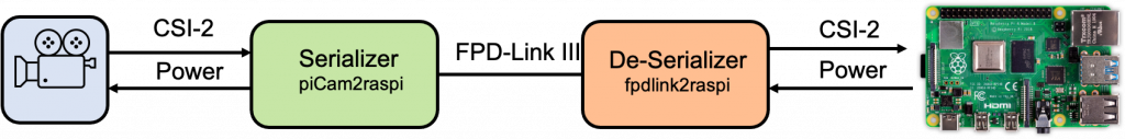
Using artificial intelligence algorithms, specifically neural networks on microcontrollers offers several possibilities but reveals challenges: limited memory, low computing power and no operating system. In addition, an efficient workflow to port neural networks algorithms to microcontrollers is required. Currently, several frameworks that can be used to port neural networks to microcontrollers are available. We evaluated and compared four of them:
The frameworks differ considerably in terms of workflow, features and performance. Depending on the application, one has to select the best suited framework. On our github page we offer guides and example applications which can help you to get started with those frameworks!
The neural networks that are generated with all those frameworks are static. This means that once they are integrated into the firmware they cant be changed anymore. However, it would be beneficial if the neural network running on the microcontroller could adapt itself to a changing domain. We developed an algorithm (emb-adta) which could be used for unsupervised domain adaptation on microcontrollers. The prototype python implementation is also available on github!
Due to their hardware architecture, Field Programmable Gate Arrays (FPGAs) are optimally suited for the execution of machine learning algorithms. These algorithms require the calculation of millions or even billions of multiplications for each input. To successfully accelerate a neural network, parallel execution of multiplication is the key. The obvious suggestion for parallel execution is a Graphics Processing Unit (GPU), offering hundreds of execution cores. For years, GPU vendors have been adapting the capabilities of their GPUs to meet the demand for narrow integer and floating-point data types used in AI. But still, a GPU will execute one Neural Network (NN) layer after the other, with data transfers between computation cores and memory.
Implementing Neural Networks in FPGAs has several advantages:
Flexible bit widths for both integer and fixed-point data types.
Large numbers of scalable hardware multiplier cores.
Flexibility due to tightly coupled memory blocks with wide parallel interfaces, allowing access to vast numbers of data points in each clock cycle.
Considering the previous points, the FPGA clearly provides all the resources required for highly parallel execution of NN algorithms.
Existing
frameworks
Unfortunately,
the act of porting a trained network to HDL code for implementation in the FPGA
is not trivial. FPGA vendors have started to provide frameworks for running NNs
in their devices. These include HDL-coded NN-coprocessor cores as IP blocks and
matching compilers to convert a trained NN into a binary executable which will
run on the coprocessor. However, these frameworks are based on a specific
software library and therefore require a processor core running an operating
system and controlling software. This means that the NN input data and network
parameters are transferred from the software to the coprocessor in order to
calculate the output of the NN. The output values are then transferred back to
the software for interpretation.
This is
substantial overhead, especially if the input data is sampled or preprocessed
in the FPGA fabric. It would be preferable to implement the neural network
entirely in the FPGA fabric, capable of running independently from software.
ZHAW
Native Neural Network
The ZHAW
Native Neural Network (ZNNN) framework is aimed at the following goals:
Input may be received directly from FPGA fabric
Inference independent of CPU and software
Minimal latency
Maximal throughput
No access to DRAM required
With these
goals in mind, it is obvious that we trade in flexibility to gain performance
and simplicity. The NN is implemented as a rigid block, designed for one single
NN application. To allow for minimum latency, we use dedicated multipliers for
each neuron, and each layer has its own memory block for the weights and
biases. Ping-Pong buffers allow to process one input vector in one layer while
receiving the next input vector. With this structure, pipelining delays can be
minimized to the execution time of the largest layer.
Our framework will take as input a structured text file with a description of the NN, including number of inputs, data-bit widths, fix point precision, number of neurons per layer for fully connected layers, number of filters and kernel size for convolutional layers, max pool and flatting layers. From this configuration file and a training and verification data set, it will generate:
Input A trained NN model
A behavioural model written in C programming language to generate a data set for verification of the VHDL code in simulation
A test bench for verification
The VHDL code of the NN ready for instantiation in your design.
Dedicated
multipliers for the neurons will use a significant amount of the available
resources and it must be noted that larger networks will require considerably
larger devices. This will not be suitable for all NN applications. Our ZNNN
framework is optimally suited for applications such as industrial machine
surveillance where only small networks will meet the latency requirements while
still achieving the required accuracy.
Performance
A direct
comparison of ZNNN with the Deep Learning Processing Unit (DPU) coprocessor
from Xilinx shows that both have their justification, depending on the
application at hand:
If you need
to run multiple, different neural networks on your FPGA with a fair
performance, you should go with the Xilinx solution. The DPU allows to process
different NN on the same implementation but is restricted to
software-controlled operation.
If
performance is essential and your application needs a single neural network,
you should use the ZNNN.
The amount
of resources in a Xilinx Zynq UltraScale+ EG9 device used by the different
solutions is shown in the following table. The ‘Xilinx DPU’ will always use
roughly the same amount of resources (depending on its configuration). It can
process various neural networks, including very large ones, with a trade-off in
throughput and processing time (latency). The resource requirements of ZNNN
strongly depend on the size and type of NN you implement. ‘ZNNN MNIST’ is a NN
with only dense layers, trained for the well-known MNIST example. MNIST is a NN
application that recognizes handwritten numbers. ‘ZNNN CONV’ is a NN using
1D-convolutional layers for non-linear signal processing in an industrial
application which accepts 64 data points as input. ‘ZNNN VIS’ is a dense
network with 2304 inputs and one single output, used for an industrial
application. According to the large number of inputs, the number of multipliers
required is very large.
NN
LUT
BRAM
DSP
Throughput (FPS)
Xilinx DPU
47
k (17%)
132 (14%)
326 (13%)
2.5 k
ZNNN MNIST
34
k (12%)
182 (20%)
947 (37%)
8510 k
ZNNN CONV
20
k (7%)
124 (13%)
712 (28%)
291 k
ZNNN VIS
87
k (32%)
182 (20%)
2467 (98%)
4081 k
Throughput of a NN can be measured in the number of inputs processed per second (FPS). On the Xilinx DPU, the whole NN is processed for one set of input data before the next set can be passed. Our ZNNN framework implements layer pipelining, meaning that as soon as the first layer is processed, the next input set can be accepted as shown in the following figure.
The latency
is slightly increased because not all layers have the same processing time, but
all the layers are processed in parallel. In return, the delay between two
inputs is greatly reduced, allowing to process more FPS. Because ZNNN includes
all the required weight parameters in the design, these don’t need to be loaded
into the FPGA at runtime. This allows to increase the FPS by orders of
magnitude in comparison with the Xilinx DPU.
Conclusion
Both the power and the cost of ZNNNs become visible in comparison with the
DPU: The DPU offers the flexibility to run various NNs on one implementation,
including larger NNs like Resnet50. The DPU is controlled by software and
therefore requires a CPU running a Linux operating system. ZNNN implementations
are ideal for small NNs and run independently from software, take their input
directly from FPGA and process orders of magnitude faster than the DPU!
The ZNNN
framework is suitable for low latency, high throughput execution of small
convolutional and fully connected NNs. It generates VHDL code for a specific NN
implementation in FGPA without the development overhead of hand-written HDL
code and testbenches. The processing performance of the ZNNN is orders of
magnitude faster than Xilinx’ DPU thanks to a high level of pipelining.
We are aware that the ZNNN implementation can require more FPGA resources than the DPU, but there are industrial applications where this approach is a perfect fit and the achieved performance meets the requirements. With the ZNNN running independently of CPU and software and the input data coming directly from the FPGA fabric, we have principally no bottlenecks in the design.
Our team will continually improve the ZNNN framework by making trade-offs between resource requirements and performance configurable.
A computer with a GPU combined with an FPGA is a powerful tool for high speed video processing. An FPGA can preprocess multiple video streams in realtime and then send the data to the GPU for further processing.
FPD-Link III is a cost-effective solution for high speed video transmission. It has made a name for
itself for its widespread use in the automotive industry. The transmission can be done over a simple
coaxial cable but includes not just a video data stream, but also a bidirectional configuration channel
and a power supply for the camera.
The purpose of this project is to design hardware which makes it possible to take full advantage of the developed FPGA-GPU co design [1] and to combine it with an FPD-Link III interface. The resulting baseboard utilizes PCI Express implemented in an FPGA which allows connecting up to 6 FPD-Link III. The FPGA is embedded in a system-on-chip and could potentially also be used stand-alone. As a further video source option, it also includes two connectors for MIPI CSI cameras. These are designed to be compatible with RaspberryPi cameras.
In a standard computer, PCI Express (PCIe) offers the possibility for two devices to exchange data on up to 16 high speed data lanes. The CPU is master of the PCIe interface and therefore usually initiates data transfers. This causes overhead and limits the maximum transfer speed for certain applications. The paper FPGA-GPU Codesign from xxx implements solutions to transfer data directly from an FPGA over PCIe to a GPU without the CPU being a bottleneck for the data througput. This approach can be especially useful for applications with high resolution video streams which need to be processed in real time. Live video streams from multiple cameras can be preprocessed in the FPGA and then be transmitted via PCI Express to the GPU for further processing. This thesis is about implementing hardware suitable to take full advantage of this idea.
The goal is to be able to connect multiple cameras to a computer via a PCIe baseboard with an FPGA. The camera interface chosen for this baseboard is FPD-Link III.
FPD-Link III
FPD-Link III is a cost-effective solution for high speed video transmission. It has gained relevance in
automotive applications. Cameras in cars are becoming more common. Nowadays even low cost cars
come with a rear camera to assist while parking. FPD-Link III can also be used in different industrial
applications, especially for real time use-cases which require high-bandwidth transmissions.
The goal of this project is to develop a Baseboard that makes it possible to connect multiple FPD-Link III cameras to a standard computer with high data rates. The video data from the cameras should be preprocessed in the FPGA and then be forwarded to the computer via PCI Express. Cameras also require to be configured. This configuration will be handled in the FPGA over FPD-Link III.
The Basics of FPD-Link III
Flat panel display link III (FPD-Link III) can be used to receive data from a camera or to send data to a display. The well known standards for high speed video transmission on the consumer market are HDMI, DisplayPort and USB. However, these cables are expensive and better suited for short distances. FPD-Link III can be used with coaxial or a shielded twisted-pair (STP) cables. A 15 m coaxial cable supports data rates up to 6 Gbps and a 10 m long STQ (shielded twisted quad) cable supports up to about 5 Gbps. But FPD-Link III does not only transmit video data. In addition to the video channel, there is also a bidirectional control channel. This is needed for a processor to configure the camera sensor. In case of a display, the control channel can for example be used to send commands from the touchscreen to the processor. The video channel occupies the frequency range between 70MHz and 700MHz whereas the control channel lies between 1MHz and 5MHz. An additional feature of FPD-Link III is Power over coax which offers the possibility to power the image sensor over the coax cable. This eliminates the need for a further cable for power supply.
FPD-Link III to PCIe Video Pipeline
As shown in the figure below, the video is transmitted from a camera sensor to a serializer which sends the video over FPD-Link III in a coaxial cable to the deserializer. The deserializer transmits the data to the FPGA over MIPI CSI-2 D-PHY. In the FPGA, the data can be preprocessed and then be sent over PCIe to the memory on the computer. There will be multiple deserializers on the baseboard so multiple cameras can be connected.
The concept of the Baseboard
The following figure shows a sketch of the concept for the baseboard. The path of the video data is colored in bright green. On the left side there are six coax connectors for the FPD-Link III interface (number of coax connectors is limited to six because of the defined maximum width of a PCIe card). The data goes through the deserializer to the FPGA. From the FPGA the data is transmitted to a computer over PCIe. In addition to the FPD-Link III connectors there are two MIPI CSI-2 D-PHY connectors which are compatable with the RaspberryPi-Camera. This gives the user an additional option for a video source.
The main focus of the project is the deserializer for FPD-Link III, the integration of a SoC FPGA and the PCIe interface. The company Enclustra offers a selection of SoC modules which entail a Xilinx MPSoC (Multiprocessor system-on-chip), SDRAM, flash memory and more. The module can be mounted to the baseboard via connectors. The figure above shows additional hardware and interfaces which are needed for an operating baseboard. The SoC needs a JTAG interface for programming and debugging. An SD-card slot is added and can be used as the boot device. The boot mode switch can be used to change the source device for the boot process. The SoC can be reset over a button and a status LED gives further information about the state of the SoC. The UART (Universal Asynchronous Receiver Transmitter) is needed for the console output of the processor. An ethernet connector makes it possible to get access to the processor with SSH (Secure Shell).
A power switch makes it possible to choose between an external power supply or the 12V supplied
over the PCIe interface from the computer. The external supply is needed when the SoC should be
programmed before the computer is booted. The connection to PCIe devices are established while
booting in the bios, which means the FPGA should be programmed before the computer turns on. The
external supply is also useful when the board consumes more power than the computer can supply.
PCIe can be used in four different lane configurations: 1-, 4-, 8- or 16-lanes. The PCIe switch is used to choose between these options.
FPD-Link III DeSerializer
The deserializer converts the FPD-Link III signal to MIPI CSI-2 which can be connected to the FPGA. Texas Instruments (TI) offers a variety of solutions for FPD-Link III serializers and deserializers. The requirements for choosing a deserializer are the following:
• Input: FPD-Link III LVDS
• Output: MIPI CSI-2
• Able to connect to 2+MP (mega pixel) cameras
TI provides two deserializers which meet the given requirements. These are DS90UB960-Q1 (960) and DS90UB954-Q1 (954). The 960 and 954 models have the same maximum data rates for FPD-Link III and MIPI CSI-2. However, 954 has more GPIO pins per camera. 954 has 7 GPIOs for 2 cameras and 960 has 8 GPIOs for 4 cameras. GPIO signals are useful to get diagnostics of the deserializer, but they can also be used to connect directly to the camera sensor board. Some cameras need for example an enable signal which can be set by the processor over these GPIOs. The deserializer chosen for this baseboard is the DS90UB954-Q1. Below picture shows the available serializers and deserializers from TI
Implementation of the Deserializer
The DS90UB954-Q1 deserializer can be used with one or two camera sensors over FPD-Link III. It supports 2MP@60fps and 4MP@40fps cameras. The two input channels RIN0/RIN1 can be enabled and disabled through registers of the deserializer (Register: RX_PORT_CTL, 0x0C). The input channels can be used as single ended (coaxial channel) or as differential (STP). This baseboard uses single ended coaxial connections. This means the RN- port of a channel is connected to ground with a 15nF-capacitor and a 50 ohm resistor. The RN+ port is connected to the conductor inside the coax connector with a 33nF capacitor in series. This capacitor blocks the receiver ports of the deserializer from any DC voltage. This is especially important if power over coax is used. Power over coax (PoC) makes it possible to use the coaxial cable to supply power to the camera sensor. The output of a power supply is connected to the coaxial connector with a filter in series. This filter is needed to shield the power supply from the AC signal transmitted between deserializer and camera sensor over FPD-Link III.
Typically, the PoC voltage is between 5V and 36V baseboard. Before connecting a camera to the baseboard it must always be checked what PoC voltage is tolerated by the camera board. If needed, the PoC voltage can be cut off from the coax connector design provided from TI.
The FPD-Link III PCIe baseboard was successfully designed and produced. Parts of the baseboard
are tested and verify that the baseboard as such is functional. The components for the MPSoC are
working properly and the baseboard was successfully detected over PCIe. Some tests showed that
there is still work to do in the bring-up of the baseboard.
A task that is still open is the debugging of the PCIe to get a working link with lane width of 8 and 16. The link to a PCIe device is established during the boot of the BIOS (basic input/output system) which is demanding to debug.
Conclusion
Once all these individual parts are completed, they can to be combined into one single system that
collects video streams from multiple cameras and transfers the data to a computer via PCIe.
By Philipp Huber, Hans-Joachim Gelke, Matthias Rosenthal
GPUs with their immense parallelization are best fitted for real-time video and signal processing. However, in a real-time system, the direct high-speed interface to the signal sources, such as cameras or sensors, is often missing. For this task, field programmable gate arrays (FPGA) are ideal for capturing and preprocessing multiple video streams or high speed sensor data in real time. Besides the partitioning of computational tasks between GPU and FPGA the direct communication between GPU and FPGA is the key challenge in such a design. However, since the Data communication is typically controlled by the CPU, this often becomes the bottleneck of the system
This blog shows a new method for an efficient GPU-FPGA co-design called Frame based DMA (FDMA) which is based on GPUDirect, but without using the CPU for data transfer. This versatile solution can be used for a variety of different applications, where hard real-time capabilities are required. The Institute of Embedded Systems, an entity of Zurich University of Applied Sciences (ZHAW), developed the FDMA methodology for direct data transfers between the FPGA and the GPU. This IP has been compared with an implementation based on the Xilinx XDMA IP.
GPUDirect DMA in NVIDIA Devices Nvidia Quadro and Tesla GPUs support GPUDirect RDMA mapping of GPU RAM to the Linux IO-memory address space. The CPU and other PCIe devices can access the mapped memory directly. Using GPUDirect the FPGA has direct access to the mapped GPU RAM.
XDMA Implementation from Xilinx This implementation is based on the XDMA IP from Xilinx. With this IP the host can initialize any DMA transfer between the FPGA internal address space and the I/O-memory address space. This allows direct transfers between the FPGA internal address space and the mapped GPU RAM. However, the host has to initialize each data transfer. As a result, an application has to run on the host, which is listening to messages from the devices. This application starts the data transfers if the devices are ready.
ZHAW FDMA Implementation For this concept of direct FPGA-GPU communication, a special DMA-IP was developed at ZHAW InES. This DMA-IP is called Frame based DMA (FDMA) and is designed to work without any host interactions after system setup. This approach uses the AXI to PCIe Bridge IP from Xilinx to translate AXI transactions to PCIe transactions. FDMA supports multiple RX and TX buffers in the GPU. This allows using one buffer for reading or writing and the other buffers for GPU processing. Each GPU buffer has a flag in the GPU RAM. This flag indicates who has access to this buffer and is used for synchronization between the GPU and the FPGA.
Achieved Data rates of FDMA Implementation For the following measurements, a Xilinx Kintex 7 FPGA with PCIe Gen2x4 and an Nvidia Quadro P2000 PCIe Gen3x16 have been used. The data rates with the two implementations have been measured with the Xilinx Kintex-7 FPGA and the Nvidia Quadro P2000. The slowest link between them is PCIe Gen2x4 with a link speed of 16Gbit/s. The Figure 4 shows the average data rate for different transfer sizes. FDMA is faster for small transfers, because the host doesn’t have to initialize every transfer. For larger block sizes the XDMA implementation is faster, because of performance issues in the Xilinx AXI to PCIe Bridge IP.
Resulting Transaction Jitter FDMA vs. XDMA For real time data processing a low execution jitter is needed. This execution jitter was measured with both implementations by measuring the transfer rate of 10’000’000 data transfers of 32 bytes. Based on these measurements, the three distributions shown in Figure 5 to 7 have been calculated
As these measurements reveal, the XDMA implementation has a huge transaction jitter. This is the case because the Linux host has to initialize every single transfer and Linux is not a real time operating system. The two measurements of the FDMA implementation reveal that there is still a small transaction jitter when the X11 server is running on the same GPU but it disappears nearly completely when disabling the X11 server, as shown in the drawing below.
Conclusion Both
implementations, FDMA and XDMA make use of the direct transfers between
the FPGA and the GPU and therefore reduce the load on the CPU. The FDMA
developed at Institute of Embedded Systems does not need any host
interaction after setup and such transfer jitter is extremely low. This
makes the FDMA implementation perfect for time critical
streaming-applications.
For further information please contact hans.gelke@zhaw.ch or matthias.rosenthal@zhaw.ch
IntEdgPerf is a new benchmark for running machine learning algorithms on embedded devices. It was developed at the Institute of Embedded Systems (InES) at the Zürich University of Applied Sciences. IntEdgPerf is a framework that allows a fair comparison between different embedded processors that can be used for executing neural networks.
The area of embedded AI is a quickly emerging market where many hardware manufacturers provide accelerators and platforms. So far, metrics and benchmarks provided by the manufacturers are not usable for comparison.
IntEdgPerf incorporates a collection of multiple TensorFlow AI models. It measures the time for the computations of the machine learning algorithm on embedded devices. The benchmark is dynamically extendable by allowing new machine learning models to be integrated. Hardware specific calls can be implemented as modules and integrated in the benchmark.
The benchmark was verified on multiple processors and machine learning accelerators such as Nvidia Quadro K620 GPU, Nvidia Jetson TX1 & TX2 and an Intel Xeon E3-1270V5. Also hardware accelerators, without a direct interface to TensorFlow, such as the Intel Movidius Neural Compute Stick were benchmarked. All tests used unoptimized networks and systems.
The following convolutional models were used in the test:
CNN3: This is a fully convolutional neural network, using only convolutional layers. Instead of using maxpool-layers a stride size of two is used to decrease size (the stride size defines the pixel shift of the convolution filter).
CNN3Maxpool: The effect of maxpool on the performance is shown by comparing the previously described network to the same version, utilizing maxpool instead of stride sizes higher than one.
CNN2FC1 and CNN2MaxpoolFC1: A third and fourth comparison can be made when replacing the last layer of the two previous networks with a fully connected layer. This allows more flexibility for the network for the input size of the image.
We have developed a simple software to show how a custom keras model can be automatically translated into c-code. The generated c-code can, in combination with the ARM-CMSIS-NN functions, be used to run neural-net calculations in an efficient way on an embedded micro-controller such as the CORTEX-M4.
The HDMI2CSI board for capturing 4K HDMI was ported to the latest release of L4T (28.2.1) including the bug fix in the Nvidia VI (see forum: [1], [2]). Major differences where adapted from L4T 28.1 to L4T 28.2.1 and our developed hardware is again able to capture 2160p30. Run the tc358840 outside its specification (>1Gbps) you could also capture 2160p60.
If you are running into problems capturing after a format change restart your application. Currently the Nvidia VI does not recover from an error, namely PXL_SOF syncpt timeout.
The NVIDA Tegra™ Processors TX1/TX2 with their powerful GPUs are ideal for use in professional audio mixing consoles or audio video equipment. However, if multiple audio channels are required, the TX1/TX2 is limited to I2S audio inputs. Utilizing the MIPI® Camera Serial Interface (CSI-2) and the InES I2S to CSI-2 converter IP, enables streaming of up to 256 digital audio channels into the TX1/TX2.
Institute of embeddeded Systems (InES) developed an FPGA-IP which converts the I2S audio to up to four CSI-lanes for feeding audio into mobile processors like the NVIDA Tegra™ TX1/TX2.
A Linux driver, which links the received CSI signals to the Tegra™ TX1/TX2 processor buses, is also available. Hence, audio can be processed on the TX1/TX2 GPU or the internal audio blocks.
I2S sources could be audio codecs, SDI or HDMI chips. The CSI-2 protocoll engine can be configured to generate CSI-2 data packets for one or four CSI lanes, depending on the required bandwidth. The CSI clock and data physical interfaces support differential (high speed) and low power CSI-2 signals.
The IP is written in VHDL and tested with Intel Cyclone-IV FPGAs. It is also possible to be synthesized into Xilinx or Lattice FPGAs.
For more information contact Hans-Joachim Gelke (hans.gelke@zhaw.ch)
Embedded devices like the Nvidia Tegra X1/2 offer tremendous video processing capabilities. But often there are bottlenecks hindering you from taking advantage of their full potential. One solution to this problem is to employ the general purpose compute capabilities of the GPU (GPGPU). For this purpose, we have developed a GStreamer Plug-In that lets you add a customized video processing functionality to any pipeline with full GPU support.
A possible application is shown in the image below. Two video inputs are combined to a single video output as a picture-in-picture video stream. A 4k image is depicted in the background and on top of it a downscaled FullHD input is streamed.
In order to cope with the huge amount of data, the video processing is outsourced to the GPU. The use of CUDA allows you to create new algorithms from scratch or integrate existing libraries. The plugin enables you to benefit of the unique architecture of the TX1/2, where CPU and GPU share access to the same memory. Therefore, memory access time is reduced and unnecessary copies are avoided. The next image shows a pipeline of the example mentioned above.
At the beginning of the pipeline, where the data rates are the highest, the GPU and internal Hardware encoders are used. The CPU can then handle the compressed data easily and gives access to the huge number of existing GStreamer Plug-Ins. For example it is capable of preparing a live video stream for clients.
The GStreamer Plug-In can also serve as a basis for other applications like format conversion, debayering or video filters.
The HDMI2CSI board for capturing 4K HDMI now supports both TX1 and TX2. Video capturing is fully supported for resolutions up to 2160p30 on Input A and 1080p60 on Input B.
Driver development will continue on L4T 28.1. The previous 24.2.1 branch is considered deprecated.
Driver for tc358840: Now using the updated version that is already in the 28.1 kernel (with a small modification)
Device tree: Adapted to be compatible with 28.1 (if you come from previous L4T, please note the new way of flashing a device tree in U-Boot! Also the structure is different with separate repositories for kernel and device tree)
Vi driver: Using the new version from Nvidia instead of our implementation, since it now supports “ganged mode” for combining multiple VI ports
Custom resolutions: The EDID can be read and written from the Linux userspace (See [1]) to support different resolutions/timings on the fly
If you want to use Userptr/Dmabuf mode in GStreamer v4l2src, you still need to rebuild GStreamer. The reason is that GStreamer by default uses libv4l for the REQBUF ioctl. The libv4l implementation of this ioctl does NOT support userptr/dmabuf. But you can just build GStreamer without libv4l and it will use correct implementations for the ioctls and work.
Recent Comments