Modern SoC devices offer high performance for data analysis and processing. In order to transfer accordingly high data rates, the choices for high speed general purpose interfaces are limited. The first that comes to mind is PCIe, which is available in most high performance SoCs. However, PCIe requires a relatively complex controller on both data source and sink. Additionally the fact that PCIe is such a commonly used interface means that all of the SoCs PCIe controllers may already be occupied by peripherals.
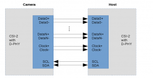
Coming from the mobile market, some SoCs additionally offer MIPI Camera Serial Interface (CSI) / Display Serial Interface (DSI) [1] interfaces, for example the Nvidia Tegra K1 / X1 or Qualcomm Snapdragon 820. These interfaces were designed for high bandwidth video input (CSI) and output (DSI). These state-of-the-art SoCs provide CSI-2 D-PHY interfaces which can have a transmission rate of 1.5 to 2.5 Gbps/lane. One such interface consists of a maximum of 4 data lanes and one clock lane. Typically, one to three interfaces are available, allowing to connect up to six different devices (depending on the SoC model).

Figure 1: MIPI CSI-2 D-PHY interface
Instead of restricting the use of the CSI/DSI interfaces to video only, we propose to use them for transferring general purpose data. The theoretical maximum bandwidth of such an implementation is 30 Gbps (using 3 4-lane MIPI CSI/DSI interfaces). For a data acquisition application, a sampling rate of 1.875 GSps can be handled. A comparable PCIe x4 v2 interface provides a maximum throughput of 16Gbps, resulting in 1 GSps sampling rate. We successfully implemented and tested digital audio data transmission over CSI/DSI and will continue to explore this interesting interface.
[1]
http://mipi.org/specifications/camera-interface