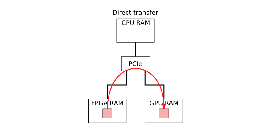
By Philipp Huber, Hans-Joachim Gelke, Matthias Rosenthal

GPUs with their immense parallelization are best fitted for real-time video and signal processing. However, in a real-time system, the direct high-speed interface to the signal sources, such as cameras or sensors, is often missing. For this task, field programmable gate arrays (FPGA) are ideal for capturing and preprocessing multiple video streams or high speed sensor data in real time.
Besides the partitioning of computational tasks between GPU and FPGA the direct communication between GPU and FPGA is the key challenge in such a design. However, since the Data communication is typically controlled by the CPU, this often becomes the bottleneck of the system

This blog shows a new method for an efficient GPU-FPGA co-design called Frame based DMA (FDMA) which is based on GPUDirect, but without using the CPU for data transfer. This versatile solution can be used for a variety of different applications, where hard real-time capabilities are required.

The Institute of Embedded Systems, an entity of Zurich University of Applied Sciences (ZHAW), developed the FDMA methodology for direct data transfers between the FPGA and the GPU. This IP has been compared with an implementation based on the Xilinx XDMA IP.

GPUDirect DMA in NVIDIA Devices
Nvidia Quadro and Tesla GPUs support GPUDirect RDMA mapping of GPU RAM to the Linux IO-memory address space.
The CPU and other PCIe devices can access the mapped memory directly. Using GPUDirect the FPGA has direct access to the mapped GPU RAM.

Fig. 1: Direct transfer without CPU involvement

XDMA Implementation from Xilinx
This implementation is based on the XDMA IP from Xilinx. With this IP the host can initialize any DMA transfer between the FPGA internal address space and the I/O-memory address space. This allows direct transfers between the FPGA internal address space and the mapped GPU RAM. However, the host has to initialize each data transfer. As a result, an application has to run on the host, which is listening to messages from the devices. This application starts the data transfers if the devices are ready.

Fig. 2: Xilinx XDMA IP based implementation

ZHAW FDMA Implementation
For this concept of direct FPGA-GPU communication, a special DMA-IP was developed at ZHAW InES. This DMA-IP is called Frame based DMA (FDMA) and is designed to work without any host interactions after system setup. This approach uses the AXI to PCIe Bridge IP from Xilinx to translate AXI transactions to PCIe transactions. FDMA supports multiple RX and TX buffers in the GPU. This allows using one buffer for reading or writing and the other buffers for GPU processing. Each GPU buffer has a flag in the GPU RAM. This flag indicates who has access to this buffer and is used for synchronization between the GPU and the FPGA.

Fig. 3: InES frame based DMA implementation

Achieved Data rates of FDMA Implementation
For the following measurements, a Xilinx Kintex 7 FPGA with PCIe Gen2x4 and an Nvidia Quadro P2000 PCIe Gen3x16 have been used.
The data rates with the two implementations have been measured with the Xilinx Kintex-7 FPGA and the Nvidia Quadro P2000. The slowest link between them is PCIe Gen2x4 with a link speed of 16Gbit/s. The Figure 4 shows the average data rate for different transfer sizes. FDMA is faster for small transfers, because the host doesn’t have to initialize every transfer. For larger block sizes the XDMA implementation is faster, because of performance issues in the Xilinx AXI to PCIe Bridge IP.

Fig. 4: Average data rates comparing FDMA with XDMA

Resulting Transaction Jitter FDMA vs. XDMA
For real time data processing a low execution jitter is needed. This execution jitter was measured with both implementations by measuring the transfer rate of 10’000’000 data transfers of 32 bytes. Based on these measurements, the three distributions shown in Figure 5 to 7 have been calculated

Fig. 5: XDMA transfer jitter
Fig. 6: FDMA transfer jitter with FDMA and X11

As these measurements reveal, the XDMA implementation has a huge transaction jitter. This is the case because the Linux host has to initialize every single transfer and Linux is not a real time operating system. The two measurements of the FDMA implementation reveal that there is still a small transaction jitter when the X11 server is running on the same GPU but it disappears nearly completely when disabling the X11 server, as shown in the drawing below.

Fig. 7: FDMA transfer jitter when X11 Server is disabled

Conclusion
Both implementations, FDMA and XDMA make use of the direct transfers between the FPGA and the GPU and therefore reduce the load on the CPU. The FDMA developed at Institute of Embedded Systems does not need any host interaction after setup and such transfer jitter is extremely low. This makes the FDMA implementation perfect for time critical streaming-applications.

For further information please contact hans.gelke@zhaw.ch or matthias.rosenthal@zhaw.ch